PCIe Specification
PCIe pinout
- Differential signalling along receive (RX) and transmit (TX) lanes.
- Polarity of lanes can be inverted.
- Order of lanes can be reversed between host and device.
- Number of RX and TX lanes must be the same (symmetrical).
- Allows for more flexible routing in space constrained environment.
- Reference clock is provided from host for timing and synchronisation (100MHz).
- Polarity cannot be swapped.
- Supposed to be optional but is actually mandatory for almost all devices.
CLKREQis pull downed by device to request PCIe reference clock.PERSTis used to reset the PCIe link.PEWAKEis used by device to signal to host to wake up (maybe for network cards?).SMBCLKandSMBDATis the system management bus and is an I2C interface (optional?)
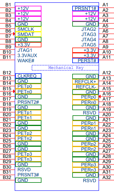
Diagram 1. PCIe x4 connector pinout
(source)
PCIe generations
- With differential signalling the fundemental frequency is half the transfer rate.
- An encoding scheme of xb/yb means X bits out for Y bits in.
- 8b/10b: 1 start bit, 8 data bits, 1 end bit.
- 128b/130b: 1 start bit, 128 data bits, 1 end bit.
| Gen | Freq (GHz) | Transfers (GT/s) | Encoding | Bitrate (Gb/s/lane) |
|---|---|---|---|---|
| 1.0 | 1.25 | 2.5 | 8b/10b | 2.0 |
| 2.0 | 2.5 | 5.0 | 8b/10b | 4.0 |
| 3.0 | 4.0 | 8.0 | 128b/130b | 7.88 |
| 4.0 | 8.0 | 16.0 | 128b/130b | 15.75 |
| 5.0 | 16.0 | 32.0 | 128b/130b | 31.51 |
Maximum design frequency
For a good eye opening the transmissions lines should be designed for 5x the fundemental frequency. For PCIe 4.0 the fundamental frequency is 8GHz which means an ideal maximum design frequency of 40GHz.
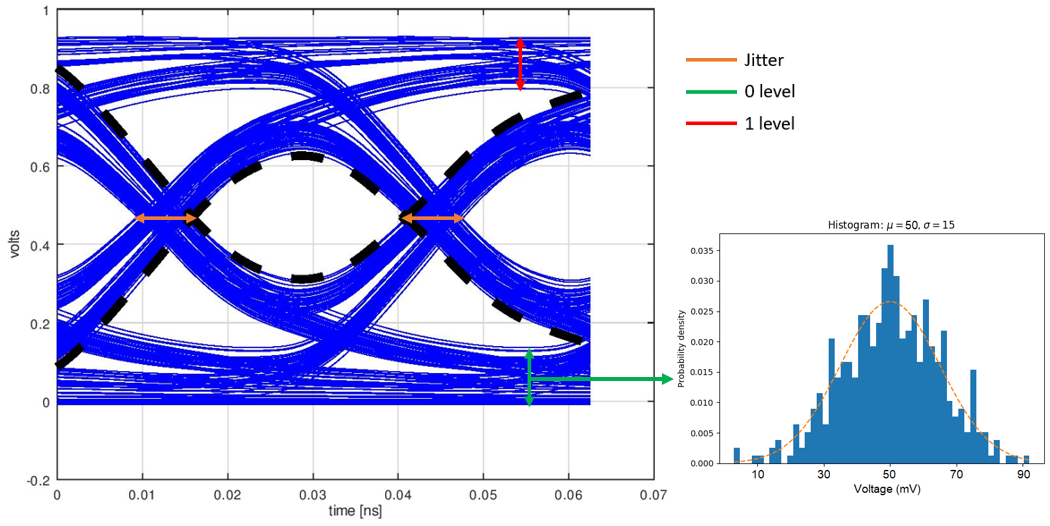
Diagram 4. Eye diagram
(source)