Via jumps
- Via jumps are necessary if a transmission line needs to switch lanes.
- In order to avoid signal reflections the characteristic impedance of the transmission line needs to remain constant when traversing from between layers through a via.
Coaxial via
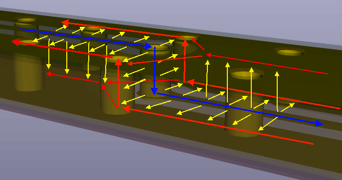
Diagram 6. Via jump with current path (red/blue) and E-field (yellow)
- If there are no nearby grounding vias then a distant current return path is used which results in a significant impedance mismatch.
- Instead we add nearby grounding vias to provide a current return path.
- This type of via structure is called a coaxial via.
- The following parameters are important when trying to control the impedance of a coaxial via:
- Distance of ground vias from signal via.
- Number of ground vias around the signal via.
- Hole size of the ground via and signal via.
- Dielectric material used to fill the vias.
Teardrop taper
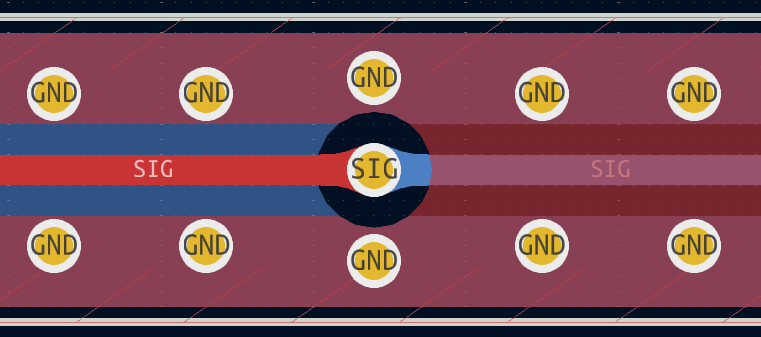
Diagram 7. Via jump design with teardrop taper
- When a signal trace goes through a via there is an impedance discontinuity especially if the trace width and via diameter are different.
- Adjusting the following can reduce the impedance discontinuity:
- Adding a teardrop taper to match trace width to via diameter.
- Adjusting the via annular diameter.
- Adjusting the via hole size.
Determining parameters
- There is no closed form equation for the impedance of a coaxial via with a teardrop taper.
- This means running a parametric search through a simulation to determine the optimal parameter values.
- Very difficult to do given the number of parameters for the coaxial via and teardrop taper which all impact performance.
- Refer to this section about simulating circuits with openEMS.
Via stubs
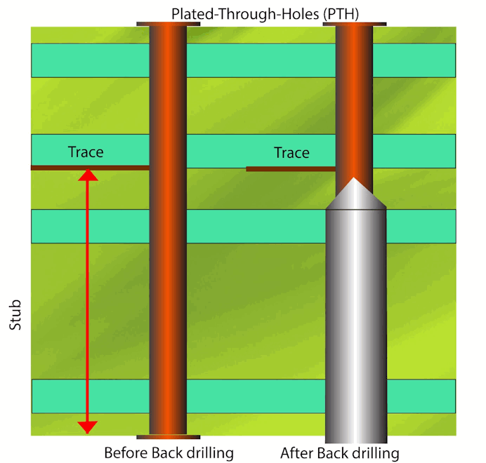
Diagram 8. Via stub back drilling
(source)
- If via jump isn’t between the top and bottom layers then there will be a stub segment in the via.
- This will have the most signficant impact at the following frequency:
\[ f_0 = \frac{c}{4 \sqrt{\epsilon_r} \times d_{stub}} \]
- Actual performance degradation happens well before this frequency.
- By decreasing \( d_{stub} \) we can increase \( f_0 \) well past our maximum design frequency and avoid problems.
- If the via stub is sufficiently short then it will not have a noticeable impact on signal integrity below our maximum design frequency.
Buried, blind and through hole vias
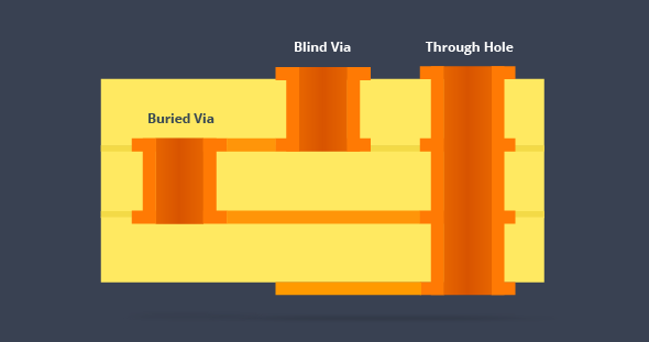
Diagram 9. Buried, blind and through hole vias
(source)
- Buried and blind vias can be used to avoid via stubs.
- These types of vias can be manufactured using a technique called backdrilling.
- However JLCPCB only supports through hole vias.