Via fence
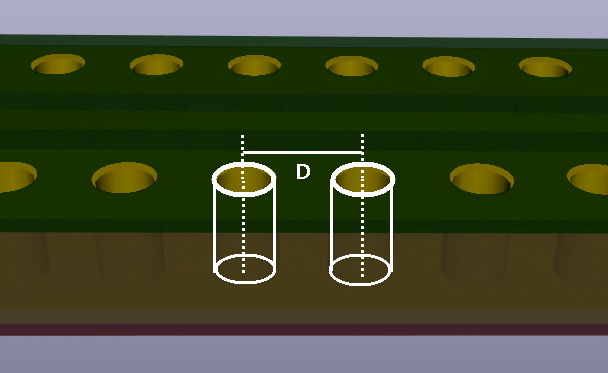
Diagram 5. Via fence
Crosstalk
- Improves impedance of coplanar ground guard trace by stitching it to a ground plane which improves E-field confinement.
- Additional ground vias improve E-field confinement.
- Both of these contribute to significantly reducing the inter-lane crosstalk.
Spacing requirements
- If spacing is incorrect it can result in worse crosstalk since fence can behave like a resonant tank.
- For a given maximum frequency which needs to be blocked, the equation is given as follows.
\[ \begin{align} d_{spacing} &= \frac{\lambda_{min}}{8} \\ d_{spacing} &= \frac{c}{8 \sqrt{\epsilon_r} \times f_{max}} \end{align} \]
For the best eye opening we should set the maximum frequency as the 5th harmonic of the PCIe fundemental frequency. The following spacing values are calculated with \( \epsilon_r = 4.1 \) for FR4.
| Gen | \( f_{0} \) (GHz) | \( f_{max} \) (GHz) | \( d_{spacing} \) (mm) |
|---|---|---|---|
| 1.0 | 1.25 | 6.25 | 2.96 |
| 2.0 | 2.5 | 12.5 | 1.48 |
| 3.0 | 4.0 | 20 | 0.93 |
| 4.0 | 8.0 | 40 | 0.46 |
| 5.0 | 16.0 | 80 | 0.23 |
Manufacturing limitations
JLCPCB has manufacturing constraints that limits the geometry of our via fence. The following values are chosen to minimise the manufacturing cost and therefore may not be the best values we can choose.
| Parameter | Type | Value |
|---|---|---|
| Via hole size | Minimum | 0.3mm |
| Via hole diameter | Minimum | 0.4mm |
| Via hole to different net distance | Minimum | 0.2mm |
| Via hole to hole spacing | Minimum | 0.2mm |
- Since we are targetting PCIe 4.0 our spacing requirement is 0.46mm and is within the manufacturing constraints.
- Our coplanar guard traces are placed 0.1mm away from signal traces so we only need 0.1mm of copper between the via and edge of coplanar guard trace.