Skin effect
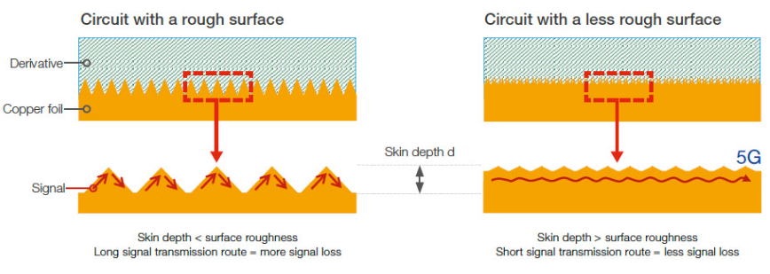
Diagram 10. Visualisation of skin effect on rough conductive surfaces
(source)
- Skin effect is when the signal current is expelled to the surface of the conductor at high frequencies.
- With a rough copper finish, skin effect can result in higher trace impedance which can result in:
- Signal loss through resistive losses.
- Impedance mismatch and signal reflections.
Increasing trace width
- Use wider tranmission line signal traces to improve impedance and therefore signal integrity at higher frequencies.
- Comes at the cost of worse impedance matching at lower frequencies.
- Signal losses generally occur at higher frequencies (via jumps, tapered transitions, skin effect, insertion loss, dielectric loss).
- Therefore to achieve best performance over the entire bandwidth we should increase transmission line width to mitigate skin effect at higher frequencies.
Copper finish
- PCB manufacturers have a variety of copper foil types to use if you need a smoother surface to avoid skin effect.
| Type of copper foil | Description | Roughness |
|---|---|---|
| Electrodeposited | Has a rougher surface on one side of the copper foil | Highest (above 1 um) |
| Reverse treated | Uses a surface treatment to reduce roughness | Moderate (0.5 um to 1.5 um) |
| Rolled-annealed | Has a smoother, denser surface from a rolling process | Low (0.25 to 0.5 um) |
| Ultra-low profile | Additional treatments are used to reduce roughness | Lowest (comparable to rolled annealed, but can be less than 0.3 um) |
- Unfortunately JLCPCB doesn’t allow you to select the type of copper foil.