Skew requirements
The PCIe standard specifies several requirements for differential pair skew.
Inter-pair skew (between lanes)
Inter-pair skew is usually not specified but has a lower bound of 1ns for PCIe 4.0.
- Assuming a propagation speed of 0.6c, the inter-pair skew is around 20cm.
- Since this is such a large value the inter-pair skew requirement is difficult to violate.
- The reason for this is because the PCIe standard states that transceivers have to do symbol synchronisation.
- Usually done with a buffer which usually can store around 20 symbols for each lane.
- For PCIe 4.0 at a transfer rate of 16GT/s, 20 symbols have a duration of 1.25ns.
Intra-pair skew (within lane)
Intra-pair skew must be less than 5 mils (0.127mm) which is rather small margin of error. The following are phenomena that can contribute to intra-pair skew and methods to mitigate them.
Bends in transmission line
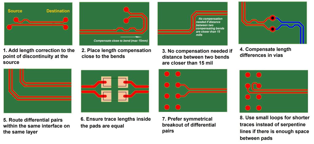
Diagram 11. Techniques to length match differential pair
(source)
- Bending causes the lengths of differential traces to become shorter and longer resulting in skew.
- Can be avoided by keeping bends short so local skew error is below 5 mils.
- If skew error is too large than it should be immediately corrected near the bend by adding serpentine bends for the shorter side of the differential pair.
- KiCAD can automatically do this using their skew correction tool.
Fibre weave effect
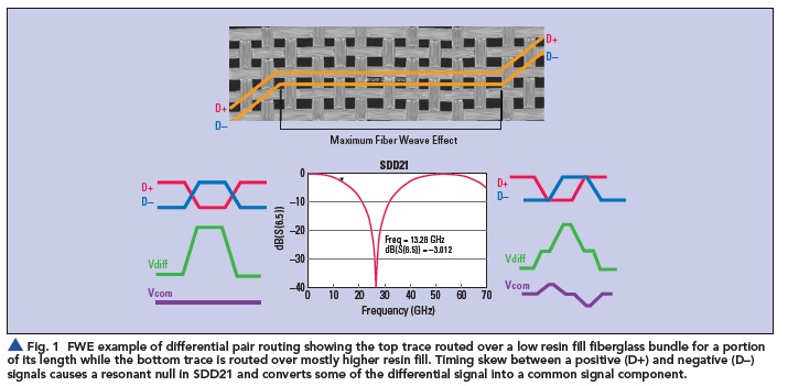
Diagram 12. Asymmetric routing over fibre-weave can produce intra-pair skew
(source)
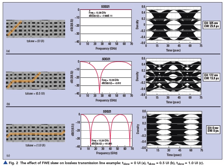
Diagram 13. Asymmetric routing over fibre-weave will degrade eye opening
(source)
- A poor choice of a dielectric with a non-uniform fibre weave pattern can result in large intra-pair skews.
- There is also no method of designing the circuit around a bad fibre weave since the manufacturer cannot position the weave at a specific offset.
Better fibre weave patterns
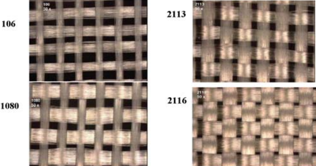
Image 13. Fibre weave patterns that are available from manufacturers
(source)
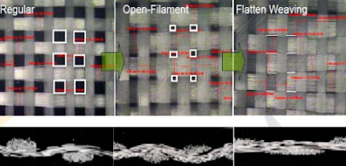
Image 14. Mechnically compressed fibre glass with flattened weave pattern
(source)
- There should be careful selection of an appropriate fibre weave pattern for maximum uniformity.
- Additionally there is also mechanically compressed fibre glass which flattens the weave and fills in any gaps to produce a uniform weave pattern.
- Here is a pdf from Isola group who are a copper clad laminate and prepreg materials manufacturer.
- It contains various high quality images of fibre weave patterns and their fill factor measurements.
- They also include treatment processes for bonding the prepreg and core to copper layers and how that effects the copper smoothness which is relevant for skin effect.
JLCPCB controlled impedance stackup
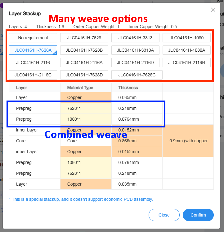
Image 15. JLCPCB fibre glass weave patterns for controlled impedance stackups
(source)
- JLCPCB offers a variety of fibre weave patterns when a multilayer controlled impedance stackup is requested (this is also free).
- It is also possible to stack two or more fibre weaves vertically to increase overall density and improve uniformity.
Hatched ground plane
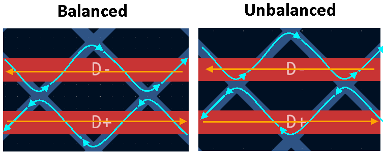
Diagram 14. Balanced and unbalanced routing of differential pair over hatched ground plane
- For hatched ground planes in a flexible pcb design asymmetric routing can produce large intra-pair skews.
- For straight transmission line routes it is trivial to route the differential pair symmetrically.
- However if the transmission line needs to bend then the hatched ground plane needs to warp to avoid introducing skew.
- This is exceptionally difficult to do with KiCAD’s built in hatched ground fill tool.
- Requires manual layout and distortion of hatched ground plane to accomodate bends in a differential pair.
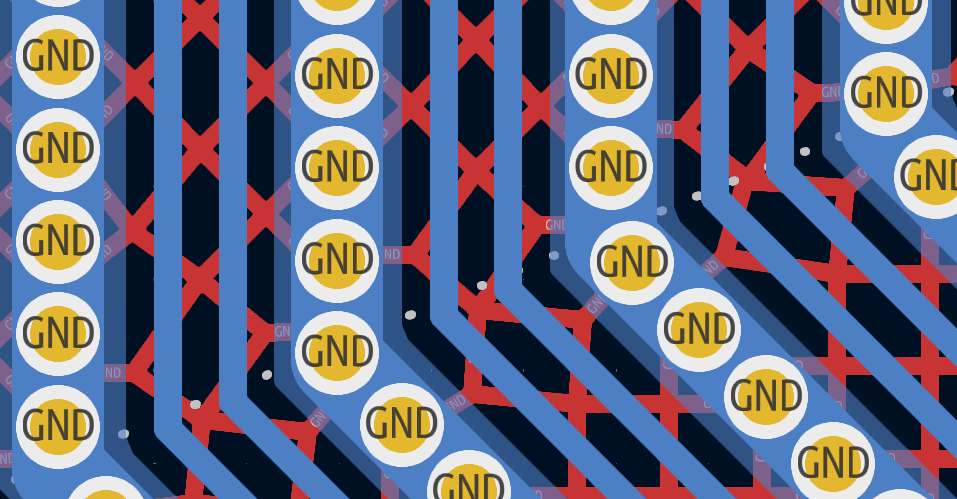
Image 16. Manually warped hatched ground plane with differential pair bend
- Unfortunately KiCAD’s built in skew correction tools cannot measure skew for hatched ground planes generated manually or automatically by their ground fill tool.
- This makes verification of the intra-lane skew extremely difficult at the design stage.