Flex connection
Type of connection
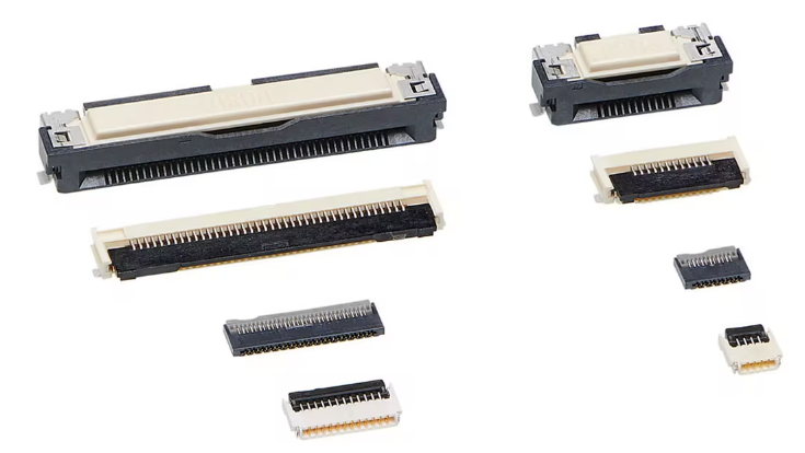
Flexible flat/printed cable connector
| Advantages | Disadvantages |
|---|---|
|
|
Soldered connection
| Advantages | Disadvantages |
|---|---|
|
|
Final choice
The soldered connection allows closer control over the design of the tranmission line and avoids the downsides of a FFC connector. This should allow us to avoid or mitigate the signal integrity issues that will arise from the use of a FFC connector.
Structure of transmission line
The following are useful equations to describe the impedance of the transmission line in relation to it’s geometry. These will be useful in determining which parameters to adjust if we want to meet our PCIe impedance target. This comes at the cost of lower modularity but is this is an acceptable compromise for higher guarantees of high frequency signal performance.
Characteristic impedance
Rough equation for a simple transmission line is given by:
\[ Z_0 = \sqrt{\frac{L}{C}} \]
This is still useful when discussing changes in impedance for a variety of transmission line structures if we discuss them in terms of differing trace inductances and capacitances.
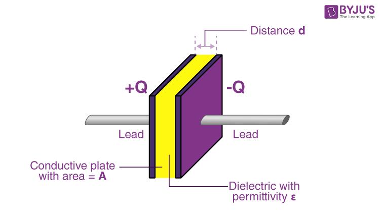
Parallel plate capacitors
The capacitance between a simple two plate system is given by:
\[ C = \frac{\epsilon_0 A}{d} \]
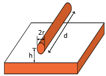
Wire over plane
The inductance of a wire over a plane can be approximated as:
\[ L = \frac{\mu_0 \mu_r d}{2 \pi} cosh^{-1}{\frac{h}{2r}} \]
Stackup height differences
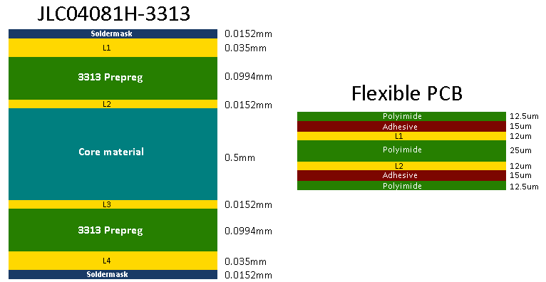
Transitioning our transmission line from an FR4 stackup to a flexible PCB stackup causes the height of the dielectric in the transmission line to significantly decrease.
- Therefore signal trace to ground plane capacitance increases which causes impedance to decrease.
- Mismatch in impedance causes signal reflections and reduced integrity.
Hatched ground plane
If the transmission line signal traces have the same width, using a suitably designed hatched ground plane will increase the impedance to meet our impedance target.
- See designing hatched ground plane for more details.
- See simulating hatched ground plane for more details.
Vertical transmission line connection
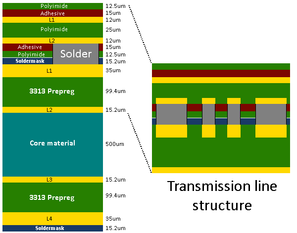
- The coplanar ground traces experience some discontinuity when it meets the solder connection due to an increase in the conductor height.
- Results in an increase in edge coupling area.
- This increases capacitance and decreases impedance.
- The E-fields between the signal traces and ground planes have to switch layers.
- Broadside coupling means stronger E-fields and more energy being carried compared to the coplanar ground traces which use edge coupling.
- Capacitive coupling is greater through a broadside connection since the traces are 0.1mm wide, compared to the edge side coupling which occurs over a 0.012mm or 0.035mm
- This was verified through an open EMS simulation.
Tapered connection
A taper is a gradual change in the geometry of a transmission line that attempts to maintain consistent impedance value across a geometric transition.
- We use a linear taper to transition the E-field broadside coupling from the ground plane on the M.2 card to the ground plane on the flexible PCB.
- A linear taper is not necessarily the best however it is very simple to design.
- Other taper designs have complex non-linear equations describing their shape which is difficult to import/design using KiCAD.
- Linear taper just requires the polyline tool in KiCAD.
Parametric optimisation of taper
To verify the performance of the taper openEMS was used.
- Simulated stackup with flex PCB connected to FR4 transmission line as a 3 layer board.
- Layers were:
[FR4 ground, signal traces, flex PCB ground]. - The soldered signal traces were approximated as an ideal single trace on a single layer.
- This was done so that only the E-field transition between the ground planes was relevant for our parametric search.
- Might not be ideal from a simulation accuracy standpoint as the geometry of the solder connection might impact the impedance match. However representing the solder connection in our simulation setup was difficult so this approximation/assumption was used.
- Layers were:
- Parametric search was done on the length, width, and amount of overlap of the linear taper.
- Shape of taper was modified separately on the FR4 stack up and flexible PCB stackup.
- Possible that simulation was not accurate since mesh size is limited and linear taper requires very small simulation grid size to accurately capture the pointy part.