Single board design
Images
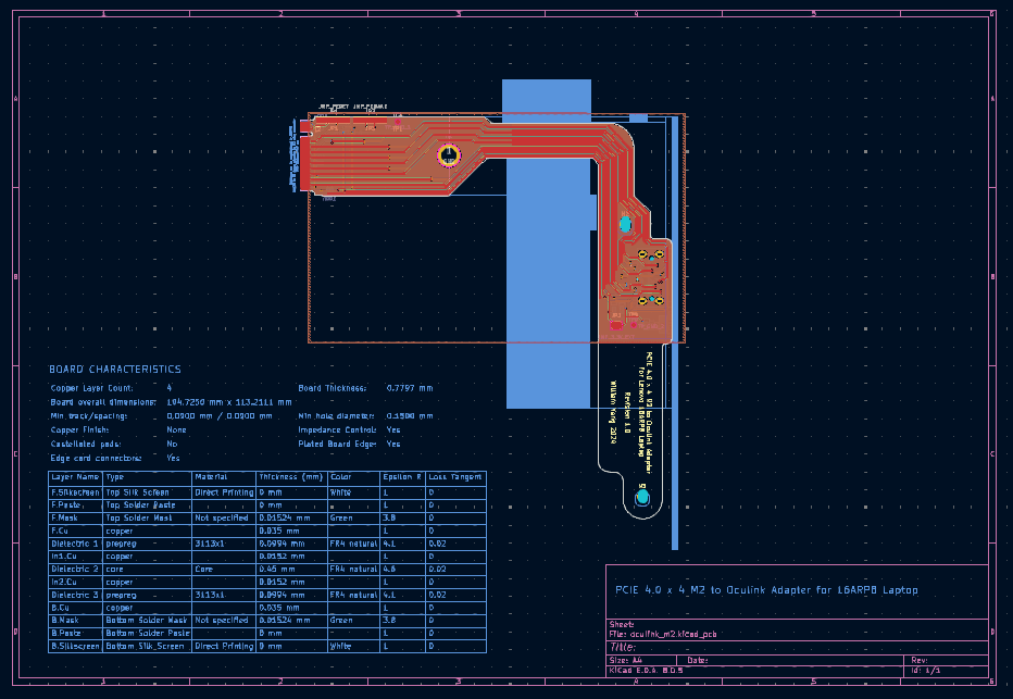
Image 9. Custom single board M.2 to Oculink adapter PCB
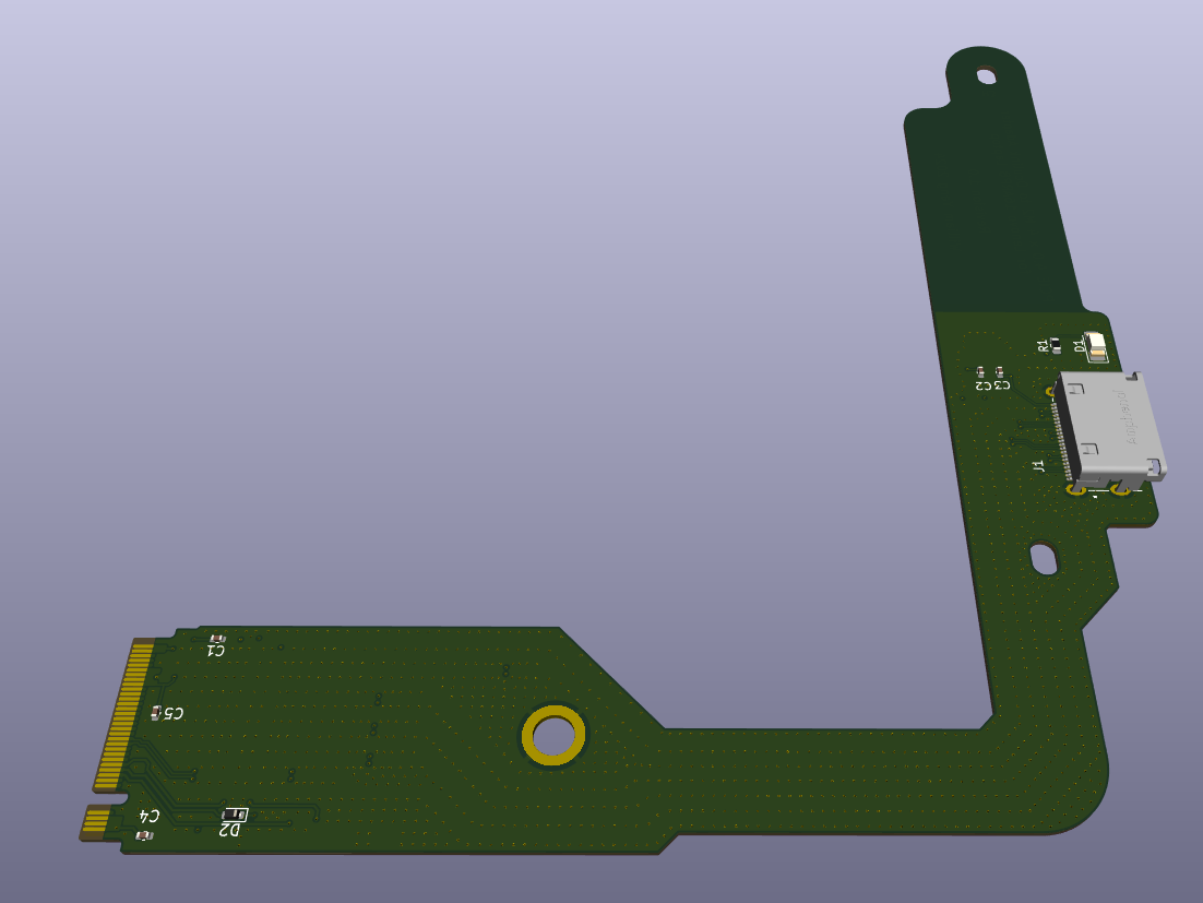
Image 10. Custom single board M.2 to Oculink adapter 3D render
Advantages
Simpler design
- Easier manufacturing and testing since we only need to solder the Oculink port and passive components.
- Single KiCAD schematic required allowing for easier design inside single project.
- Requires only a single transmission line to be designed reducing design complexity.
More reliable performance
- Having multiple boards connected over a flexible PCB adds additional potential impedance discontinuities.
- Without equipment to verify performance at PCIe 3.0+ frequencies it is difficult to validate performance.
- Introducing fewer design uncertainties will make final performance more likely to align with calculations.
Disadvantages
Narrow routing resulting in layer transition
PCIe signal lanes have to fit through a very narrow region which requires routing differential pairs onto other layers.
- Requires careful design of via jumps to prevent impedance mismatch and signal reflection.
- PCIe RX lanes have 1 via jump and PCIe TX lanes have 2 via jumps.
- Each additional via jump will worsen signal integrity so having 2 is unideal.
Port location and bending
Board has to be slightly bent so that Oculink port is at the correct height with laptop chassis.
- Might result in damage to circuit if the board isn’t flexible enough.
- Could result in degraded transmission line performance due to stretching of traces and introduction of inter-pair skew in differential pairs.
- Could result in Oculink port pad connection breaking due to uneven mechanical stress.
Long distance routing
PCIe lanes have to be routed over a moderately long distance (12cm).
- We are using FR4-TG135 which has a high dielectric loss at high frequencies.
- If we are targetting PCIe 4.0 then we need to handle the 5th harmonic of the fundemental frequency which is 40GHz.
- It is highly unlikely to maintain PCIe 4.0 over such a long distance with a high loss dielectric.
Large size
Single board design is relatively large.
- M.2 slot requires 0.8mm thickness which results in mandatory lead free HASL that costs $4.80USD.
- Exceeds 50mm x 50mm threshold meaning board goes from $2.00USD to $7.00USD.
- Exceeds 100mm x 100mm threshold meaning additional engineering fee of $24.00USD.
- Overall cost of $35.80USD.