Hatched ground
Simulation setup
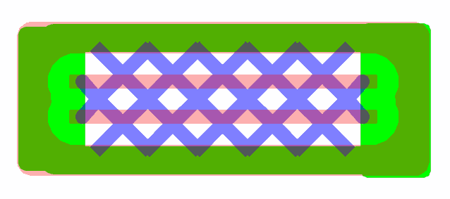
Image 19. Automatically generated hatched ground plane for openEMS simulation
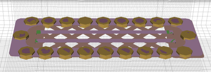
Image 20. Automatically generated hatched ground plane 3D model
- Various geometries were auto-generated by a Python script which produced image files with different hatch configurations.
- These were then given to gerber2ems to simulate using openEMS.
- A parametric search over the hatch width and gap amount for the optimum search was performed.
Parameter search
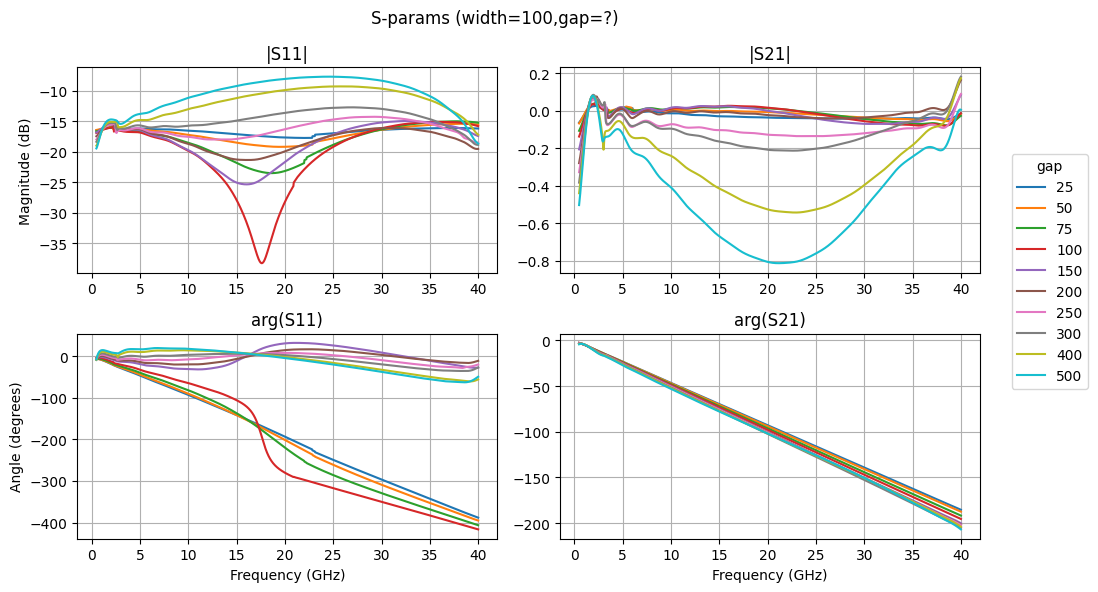
Figure 1. S-parameter results of parameterised search of hatched ground plane with a hatch width of 150um
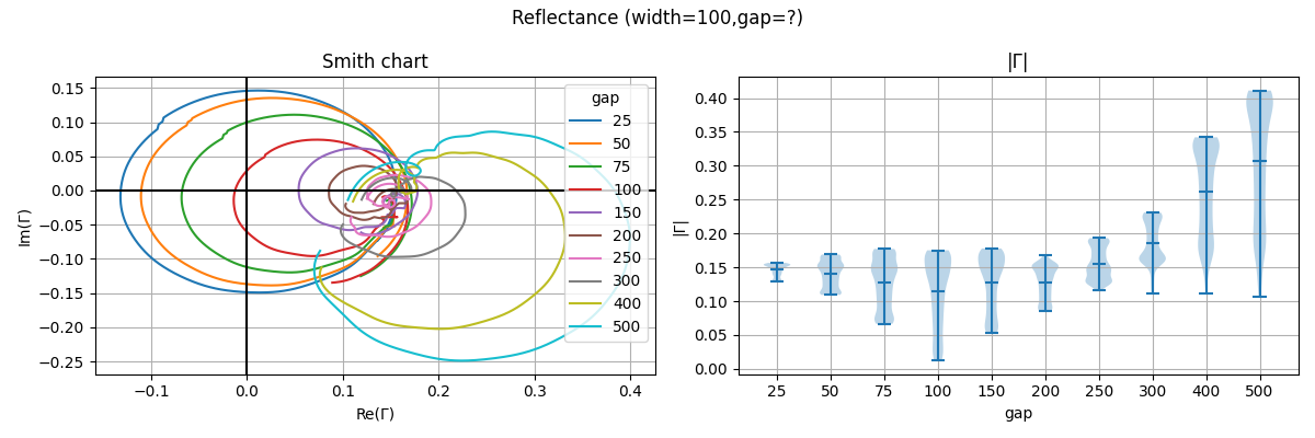
Figure 2. Reflectance results of parameterised search of hatched ground plane with a hatch width of 150um
- The configuration with the lowest mean energy loss in our frequency range of interest (0GHz to 40GHz) was chosen.
- This was repeated for a range of different hatch widths, and the optimum out of these was then chosen.
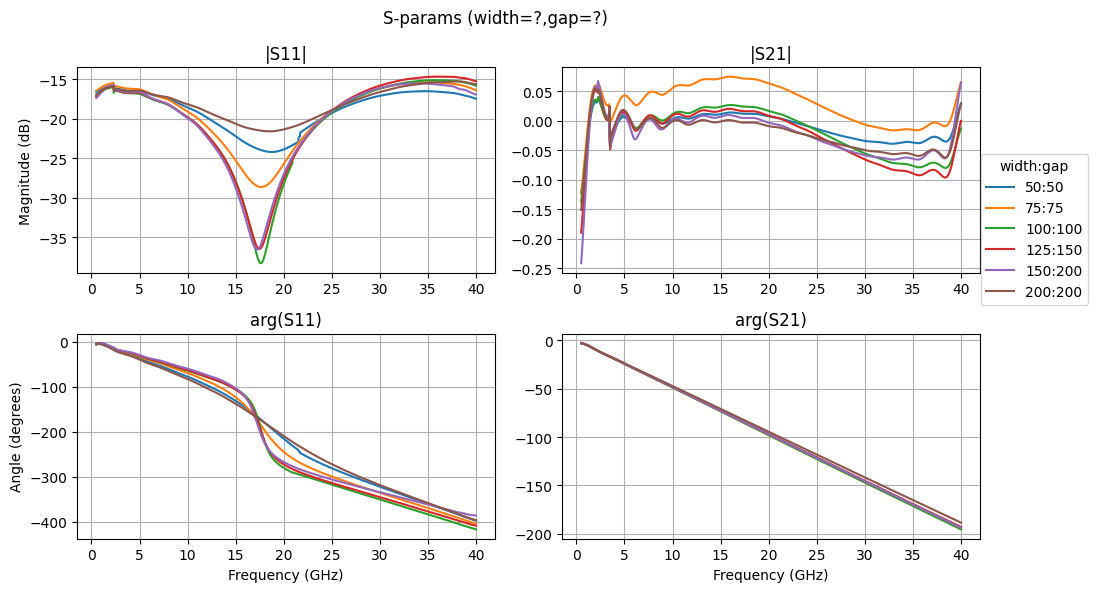
Figure 4. S-parameter results of parameterised search of hatched ground plane across all parameters
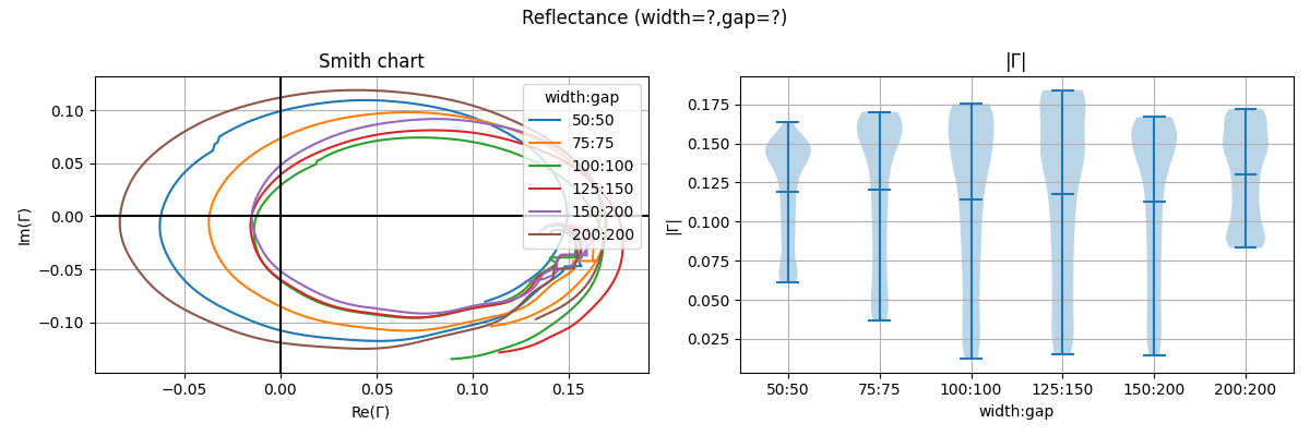
Figure 3. Reflectance results of parameterised search of hatched ground plane across all parameters
Discussion
- The average reflectance seemed to have a minimum offset of
Γ = 0.1which was probably due to the bad impedance match when transitioning from the solid ground plane to hatched ground plane in the simulation. - Highly likely that this would also occur in our flexible PCB since there is also a similar transition at the soldered connection.
- Doesn’t simulate dielectric loss or skin effect which is important for predicting how lossy the design is, especially at higher frequencies where these effects are significant.
- Right now the gerber2ems script uses a perfect conductor as the metal material, however openEMS has ConductingSheet which simulates conductivity for lossy conductors.
- Both dielectric loss and skin effect losses increase at higher frequencies however conductivity is flat across all frequencies, which makes it unsuitable for simulating these lossy effects.