Flex connector design
Images
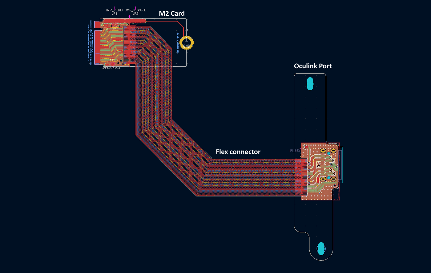
Image 11. Custom M.2 to Oculink adapter with flex connector PCBs
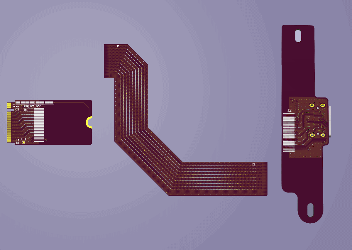
Image 12. Custom M.2 to Oculink adapter with flex connector 3D renders
Advantages
Benefits of vertical routing
- Vertical routing under M.2 2280 slot has a much wider room.
- Removes requirement to move high frequency PCIe signal traces onto a different layer.
- Avoiding additional via jumps which results in better signal integrity.
- PCIe lanes for both RX and TX have 1 via jump.
- This is an improvement for TX lanes over the single board design which have 2 via jumps.
- Allows adjustment of height offset of Oculink port for ideal positioning against side of laptop chassis.
Benefits of flexible PCB connection
Flex PCB is designed to bend unlike a fibre glass core which prevents possible damage.
- Oculink port is on separate board which doesn’t have to bend avoiding any possible mechanical damage to the SMD pad connections.
- Allows for more flexible positioning of the Oculink port if there is some error in the measurements.
Polyimide dielectric
Flex PCB uses a polyimide core which potentially could have a low dielectric loss.
- Overall length of PCIe lanes is the same but majority is over the lower dielectric loss polyimide.
- Could improve signal integrity however this is difficult to verify without proper equipment.
Flexibility of design
Easier redesign if future changes need to be made.
- M.2 card board can be kept constant.
- Flex connector can be easily redesigned and cheaply made.
- Port board can be swapped if Oculink port is damaged.
- Port board can be re-engineered to use a different PCIe compatible port like MCIO.
Lower manufacturing cost.
Cheaper overall manufacturing compared to single board design (using JLCPCB).
- M.2 card is only 22mm x 42mm which is under 50mm x 50mm threshold resulting in $2.00USD board cost.
- M.2 card is 0.8mm which means mandatory lead free HASL that costs $4.80USD.
- Oculink port board is only 21mm x 87mm which is under the 100mm x 100mm threshold meaning no additional engineering fee.
- Oculink port board exceed 50mm x 50mm threshold which means board cost of $7.00USD.
- Oculink port board can be manufactured on a stackup thicker than 0.8mm enabling HASL with lead which is free.
- Flexible PCB connector can be manufactured at $2.00USD.
- Overall cost of $15.80USD.
Disadvantages
Variability in polyimide properties
Flex PCB polyimide material comes in several varieties.
- No guarantee that the polyimide used is a low dielectric loss formulation.
- JLCPCB datasheet for their polyimide supplier shows a dielectric loss which is still substantial.
- Due to thinner stackup the electric field strength is significantly higher over a thicker stackup on FR4.
- This high E-field magnitude can result in even greater dielectric losses.
- If this isn’t offset by a low loss polyimide dielectric then the flex pcb may perform much worse than routing on FR4.
Transitioning transmission line geometry
Flex pcb requires handling transition of transmission line from FR4 stackup to flex PCB stackup.
- Requires careful design to avoid impedance discontinuities at flex PCB connection.
- Involves designing transmission line tapers to maintain impedance target across connector transition.
- Transmission line design
Transmission line design on flex pcb
Flex pcb has a very thin dielectric core for easy bending.
- Thin dielectric means transmission line needs to be designed with extremely thin traces.
- Calculations with a solid ground plane puts trace width at < 0.05mm which is not manufacturable.
- Requires using a hatched ground plane to achieve target impedance at manufacturable 0.1mm trace width.
- Hatched ground plane needs very careful design considerations and is not trivial to design.
- Hatched ground plane design
Design and manufacturing complexity
Additional complexity due to multiple boards.
- More difficult manufacturing and electrical testing due to additional soldering steps for flex connector.
- More difficult design since KiCAD doesn’t support multi-board designs necessitating multiple projects.
- Requires a more complicated project layout to support sharing of common resources like the flex connector footprint.
- Requires careful design to make sure design changes are reflected across all 3 board designs (M.2 card, flex connector, Oculink port board) to avoid miswiring.
Potential EMI issues
- Use of hatched ground plane instead of solid ground plane in flexible connector results in worse shielding at higher frequencies determined by hatch gap size.
- Since flexible pcb is routed underneath a PCIe 4.0 x 4 SSD in the M.2 2280 slot it could mean the Oculink connection will interfere with the SSD.
- Not that likely interference will be significant since the SSD also has it’s own internal solid ground plane which should shield EMI between SSD and Oculink connection.
Potential safety issue
- Flexible PCB is routed over the battery pack. In the event of a short in the Oculink connection the battery pack could be damaged and possibly ignite.
- Not that likely since PCIe connection carries low power signals and 3.3V rail isn’t used to deliver any signficant amount of power to the eGPU dock.